'BIO'logy? Huh? (,"). I used to set in my mind there will be the bad day when I see 'BIO' word. This is because I do not like Biology subject. Therefore, I drop this subject when I join matriculation program. Once again, for this week I met 'BIO's word, but it's totally different. It's about 'BIOELECTRONICS'. Fine, I love electronics but what is the relationship between biology and electronics?
OK. This week we have a talk, a special talk from Dr. Azran and he had delivered a good speech about bioelectronics. I do not know why and how he can attract me to listen on his speech about this topic. Because I thought I am going to sleep in his class (even I know I am not going to do that =D). His introduction about this topic is not straight forward to bioelectronic itself. He gave us some information about electronic first, such as electronic symbol. There are many knowledge had to apply in order to master this symbol. Electronic system has many parts to learn and I have jotted down some of it, such as:
1. Resistor colour code
 |
2. AC and DC
 |
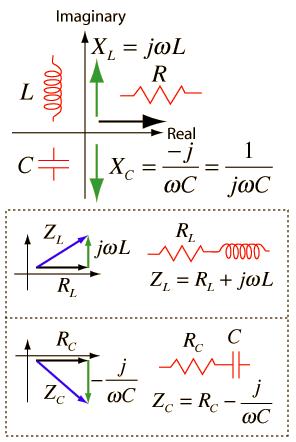
3. Impedance (Z)
 |
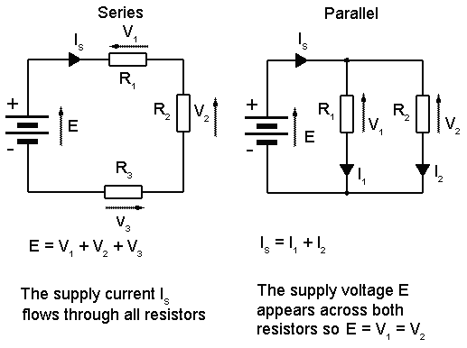
4. Series and parallel circuit
 |
5. Voltage divider (transfer function)

6. RC circuit ( low-pass and high-pass)
 |
7. Active element realization
 |
We also have to answer some problem related to series and parallel circuit including capacitors and resistors. Derivation of trigonometry functions is required to solve the problem.-->(Please mastering your M.A.T.H.S) There was also estimation method that we have to analyze in order to get it function, that is Doppler Signal Discriminator.
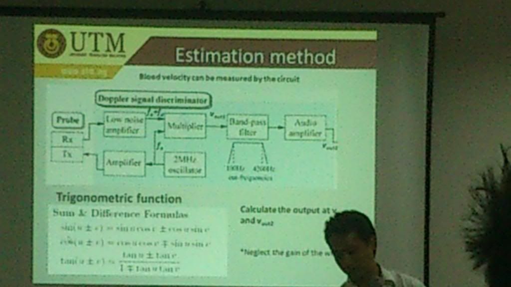 |
| Doppler Signal Discriminator |
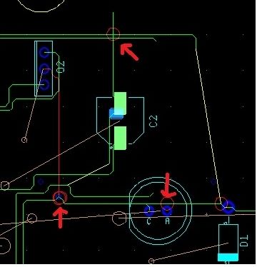
8. Probe design
 |
| Example of probe design |
Dr. Azran also had explained to us about molecular biology. The main point here is about cell staining. I do some research about this topic. What I understand is cell staining is a technique that can be used to better visualize cells and cell components under a microscope. For more information, please visit http://serc.carleton.edu/microbelife/research_methods/microscopy/cellstain.html. Here I put some pictures for cell staining :

_PAS_stain.jpg)
 |
Besides, he also shows us a video entitled 'Mechanics of Ascension'. This video tell us deeply about deoxyribonucleic acid (DNA) and its functions. There are so many DNA still not discovered yet, that also known as 'junk DNA'.
We are also introduced to a winner of Noble Prize in Medicine in 2012. He is a Japanese physician and researcher of adult stem cells .He serves as the director of Center for iPS Cell Research and Application and a professor at the Institute for Frontier Medical Sciences at Kyoto University; as a senior investigator at the UCSF-affiliated J. David Gladstone Institutes in San Francisco, California; and as a professor of anatomy at University of California, San Francisco (UCSF). Yamanaka is also the current president of the International Society for Stem Cell Research (ISSCR). For more detail about him, please visit http://en.wikipedia.org/wiki/Shinya_Yamanaka.
 |
| Shinya Yamanaka |
Lastly, we also had been explained about the use of sonication treatment to completely decellularize blood artery. I also had search some information about this. Just definition it is. Sonication is the act of applying sound (usually ultrasound) energy to agitate particles in a sample, for various purposes. In the laboratory, it is usually applied using an ultrasonic bath or an ultrasonic probe, colloquially known as a sonicator. In a paper machine, an ultrasonic foil can distribute cellulose fibres more uniformly and strengthen the paper.
Please visit http://en.wikipedia.org/wiki/Sonication for more information :) .
That's all for today. I hope I can do my best to learn more about bioelectronics. I do not care even I have to study Biology as SPM. I learn from all my lecturers that we have to struggle and strive to achieve our goal.In addition, I will not give up. Because there is a success instead hardship :)
"Although the road is long, we're going through it slowly." -Anonymous-
Thanks a lot to Dr. Azran, Dr. Kamal and En. Redzuan :)