
23/10/2012- This week we had learned how to convert from Multisim to Ultiboard. From the previous post, I had told you some about Multisim. Then this time I am going to tell you what is Ultiboard is about :) . In order to get a right information, I have done some 'googling'. Let me highlight here :
1. http://en.wikipedia.org/wiki/NI_Ultiboard:
NI Ultiboard or formerly ULTIboard is an electronic Printed Circuit Board Layout program which is part of a suite of circuit design programs, along with NI Multisim. One of its major features is the Real Time Design Rule Check, a feature that was only offered on expensive work stations in the days when it was introduced. ULTIboard was originally created by a company named Ultimate Technology, which is now a subsidiary of National Instruments. Ultiboard includes a 3D PCB viewing mode, as well as integrated import and export features to the Schematic Capture and Simulation software in the suite, Multisim.
2. http://www.ni.com/white-paper/5611/en
The NI Ultiboard interface enables efficient layout and routing of PCB designs. Integration with NI Multisim allows seamless transfer of schematics to layout. The customizable environment ensures accessibility to desired features for immediate productivity. Tools such as the spreadsheet view, toolbox and design wizards easily manage, control and define any board layout.
Part placement and copper routes are optimized to either allow full control for precise definition of critical parts or automation for quick design completion. The 3D preview renders a completed, populated board to gain a virtual perspective before production. Ultiboard exports and produces industry standard format such as Gerber and DXF to take a final, optimized board to prototype and manufacture.
The Ultiboard product editions (Full, Power Pro) provide a complete set of tools for professional PCB layout:
Intuitive, user-friendly design environment
Integrated spreadsheet view for managing design constraints, part placement, and copper routing
Easy-to-use design tools optimized for speed or precise control
Export to industry standard file formats such as Gerber and DXF for prototype and manufacturer.
In other words, Multisim and Ultiboard are closely related. Without the usage of Multisim, we cannot get the result in Ultiboard--> in form of 3D. Let me show you their closeliness :)
This is Multisim's front page :
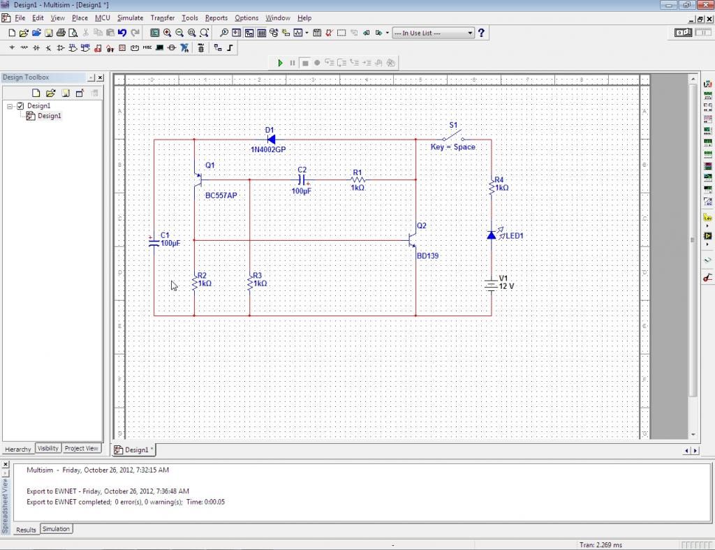
In order to convert Multisim to Ultiboard, go to Transfer button. Select 'Transfer to Ultiboard', You will have this window appear:

This window is appearing in order to tell you what component you use and to confirm the number of component that you have use. After you click 'OK' button, the next window will be like this :

This step-by-step instruction had told you how the relationship between Multisim and Ultiboard. After done these 3 main steps, you can do whatever you wish for your Ultiboard. For example, I have finished design my components in the board. Have a look at this:
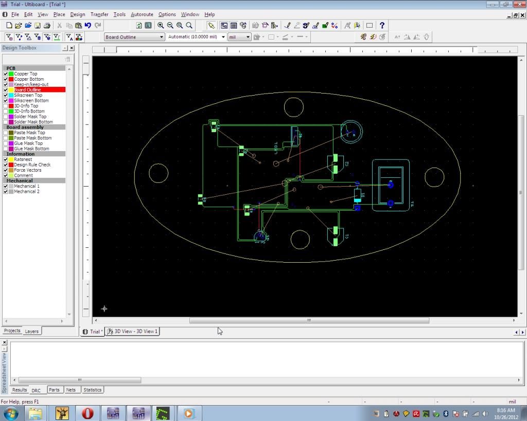
Then I convert it to 3D view. To do this, simply click 'Tools' then go to 'View 3D' button. This window will appear on your screen:

I also have captured some views from this 3D component. It included:
1. Upper view:
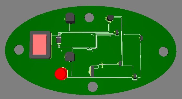 |
| Upper view of 3D's component on the board. |
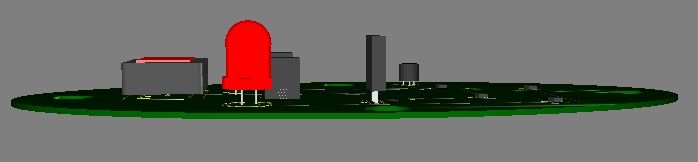 |
| Front view of 3D's component on the board |
 |
| Other side of 3D's component on the board. |
If I am not mistaken, this view is used for the soldering part. (For the next class, we will do some soldering and I cannot wait for that time! :)
There are so many things have to be consider. In order to do some replacement of component, you will face some problem. This may include wrong connection of wire, DRC error (which the connection of wire is prohibited for some areas) and many more. Try to have a look on this circuit:
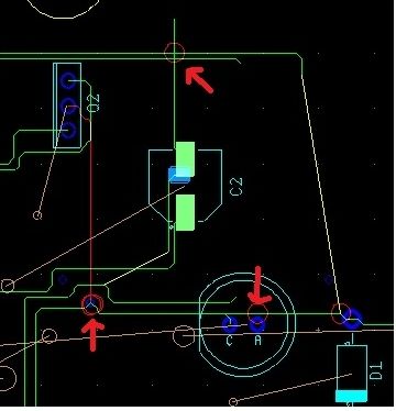 |
| Some error of DRC. |
There are so many skills you have to learn to master this software. I have learned some of it, and this is the result I have obtained :)
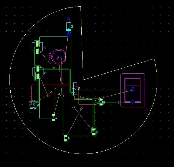 |
| Complete circuit :) |
That's all for my workshop lesson this week. I am really interested to do more skills for this software. It challenges my mind and make me feel excited to explore more :) In order to be a professional engineer that will contribute to our lovely country, I will study hard! YEAH!
- "Those who are successful are not those who failed in the attempt, not even those who often fail but those who never fail to try and keep trying until success we have achieved." - by Anonymous
Thanks a lot to Dr. Kamal and En. Redzuan :)
No comments:
Post a Comment